Low-dimensional quantum materials
Materials in a confined geometry can exhibit completely different properties in comparison with their bulk counterparts. The research effort in our group focuses on the novel phases of matter emerging from the interplay between lattice, charge, orbital, and spin degrees of freedom in the low-dimensional quantum materials. The mechanical exfoliation of van der Waals (vdW) materials and molecular beam epitaxy (MBE) growth of thin films provide a fertile ground to explore novel quantum phenomena in the low-dimensional limit. In particular, the vdW and MBE heterostructures provide high flexibility of engineering their functionalities through a variety of approaches such as strain, electric doping, external fields, and interlayer twist.
In our group, we are interested in discovering and understanding the emerging quantum phenomena in vdW and MBE heterostructures using experimental techniques based on the femtosecond laser and synchrotron radiation as follows.
Experimental techniques
Lab-based nonlinear optical spectroscopy
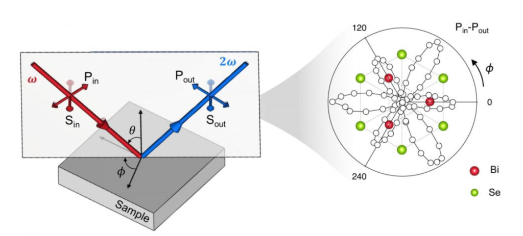
Second harmonic generation (SHG) is a laser-optical process in which the frequency of incident light is doubled through its second-order nonlinear interactions with the material. The unique feature of the setup is the rotational anisotropic experimental geometry in which the intensity of the SHG signal is measured as a function of the azimuthal angle (ϕ) of the scattering plane with tunable polarization configurations (Pin-Pout, Pin-Sout, Sin-Pout, and Sin-Sout). Based on Neumann’s principle which states that the symmetry of the susceptibility tensor must obey all the symmetry operations contained in the crystal, the rotational anisotropic SHG makes a powerful tool to detect symmetry breaking of a crystal by directly probing the nonlinear susceptibility tensor elements.
Synchrotron-based spectroscopy and microscopy
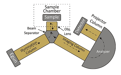
Spectroscopic photoemission and low-energy electron microscopy (SPE-LEEM) offer a versatile tool that uniquely integrates microscopy, diffraction, and spectroscopy techniques, enables real-time imaging and in situ structural, chemical, and electronic analysis of surfaces and interfaces. Meanwhile, the third-generation synchrotron radiation light source can provide a high-brightness beam with energy of 15-1500 eV and full control of the polarization of the light. Synchrotron-based SPE-LEEM has four imaging modes that allow us to extract comprehensive information from low-dimensional quantum materials:
(i) Low-energy electron microscopy (LEEM): characterize surface morphology with a spatial resolution of <20 nm.
(ii) Micro-spot low-energy electron diffraction (μ-LEED): determine local crystalline structure with a beam spot size of ~2 μm in diameter.
(iii) Photoemission electron microscopy (PEEM): surface analysis with chemical and elemental sensitivity. X-ray PEEM also enables magnetic domain imaging with x-ray magnetic circular dichroism (XMCD).
(iv) Micro-spot angle-resolved photoemission spectroscopy (μ-ARPES): probe local electronic structure with a beam spot size of ~5 μm in diameter and energy resolution of ~150 meV.
Our SPE-LEEM studies of low-dimensional quantum materials are performed using the facilities of the Electron Spectro-Microscopy beamline (ESM, 21-ID-2) at NSLS-II at Brookhaven National Laboratory, with Dr. Jerzy Sadowski.
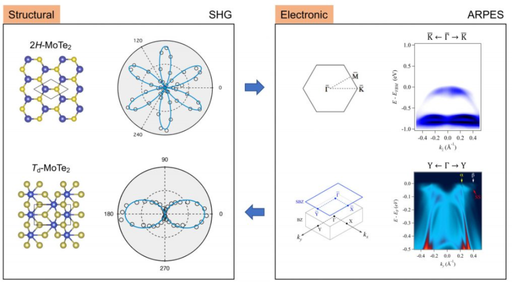
Revealing structure-property relationship through the combination of nonlinear optics and photoemission spectroscopy
The structure-property relationship is crucial for engineering and controlling the quantum phenomena to realize potential applications in optoelectronic and spintronic devices. Use polymorphic MoTe2 as an example. In the left panel, the polar plots of rotational anisotropic SHG patterns demonstrate the distinct lattice structure between the 2H and Td phases of MoTe2. The right panel displays the ARPES band maps of 2H- and Td-MoTe2, respectively. The results clearly show that polymorphic MoTe2 possesses different electronic properties: it is a semiconductor in the 2H phase and becomes metallic in the Td phase.